Editor's Pick: Measuring dielectric and electro-optic responses of thin films using plasmonic devices
This paper introduces a simple method for the measurement of the relative permittivity and the Pockels coefficient of electro-optic (EO) materials in a waveguide up to sub-THz frequencies. By miniaturizing the device and making use of plasmonics, the complexities of traditional methods are mitigated. This work elaborates the fabrication tolerance and simplicity of the method, and highlights its applicability to various materials, substrates and configurations.
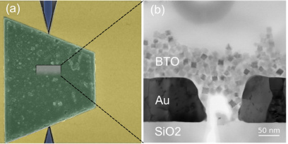
(a) A top-view SEM image of the plasmonic slot section with Si access waveguides (blue), gold contacts (yellow) and the patterned BTO nano-particles (green). In (b) a TEM cross section of a plasmonic slot is displayed.
This is a journal paper published in external pageOptics Expres.